
 英語
英語 中文简体
中文简体 Русский
 Español
 Português
 Türkçe
 العربية
 Deutsch
 Polski
 Italiano
 Français
 한국어
한국어 ไทย
ไทย Tiếng Việt
 日本語
日本語
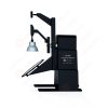
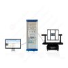
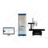

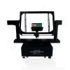
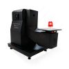
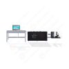











CDM ESDテストシステム
ユーザーズマニュアル
適用 LISUN models: ESD-CDM
1. Basic Understanding of the Equipment
1.1 製品概要
The ESD-CDM (Charged Device Model) CDM ESD Test System is a high-precision immunity test instrument specifically designed for “charged device contact discharge” scenarios involving semiconductor devices during production, transportation, and assembly. Its core function is to simulate the transient discharge process that occurs when a semiconductor device—which has become charged (e.g., through triboelectric charging or induced charging)—comes into contact with a grounded object. By precisely controlling parameters such as discharge voltage and current waveforms, it evaluates the device’s tolerance to this type of “latent electrostatic shocks,” enabling the early detection of risks such as internal circuit burnout and functional failure. It provides a testing basis for the reliability design, mass production quality inspection, and international compliance certification of semiconductor devices.
This system features an integrated “charge injection–contact discharge” design and is equipped with a high-precision charge measurement module, with a discharge voltage error of ≤±3%; It is compatible with fixtures for mainstream semiconductor packages such as DIP, SOP, QFP, and BGA. Equipped with a touchscreen display in both Chinese and English, it supports one-click configuration of test parameters, automated control of the discharge process, and real-time storage of test data, meeting the semiconductor industry’s requirements for high precision and high compatibility in testing.
1.2 適⽤規格
This equipment fully complies with the following domestic and international CDM electrostatic discharge testing standards:
| 標準番号 | 標準タイトル |
|---|---|
| ANSI/ESDA/JEDEC JS-002-2014 | Electrostatic Discharge (ESD) Sensitivity Testing—Charged-Device Model (CDM)—Component Level |
| IEC 60749-28:2022 | Semiconductor Devices—Mechanical and Climatic Test Methods—Part 28: Electrostatic Discharge (ESD) Sensitivity Testing—Charged-Device Model (CDM) |
| AEC-Q100-011 | Charged Device Model (CDM) Electrostatic Discharge Test |
| EIA/JESD22-C101 | Test Method for Electrostatic Discharge Sensitivity Testing—Charged-Device Model (CDM) |
| ANSI/ESDS 5.3.1-2009 | Electrostatic Discharge Sensitivity Testing – Charged Device Model (CDM) – Component Level |
| JEITA ED-4701/300 Test Method 305 | Charged Device Model Electrostatic Discharge (CDM/ESD) |
| GB / T 4937.28-2024 | Semiconductor Devices—Mechanical and Climatic Test Methods—Part 28: Electrostatic Discharge Sensitivity Testing—Charged Device Models (Equivalent to IEC 60749-28:2022) |
1.3 Principles of the CDM Discharge Model
The Charged Device Model (CDM) simulates the physical process by which a semiconductor device accumulates static electric charge and then discharges it through contact between its pins and a grounded conductor. The device becomes charged through an induced high-voltage electric field, and when the device’s pins come into contact with a ground probe, the stored charge is rapidly discharged within nanoseconds, forming a discharge current pulse with a high peak and a fast rising edge. This pulse exerts a stress on the device’s internal gate oxide layer and metal interconnects, thereby evaluating the device’s electrostatic discharge (ESD) tolerance.
2.安全上の注意
2.1 作業環境に関する要件
動作温度:15℃~35℃、動作相対湿度:30%~60%。高電圧アーク放電を防ぐため、高湿度または結露のある環境では使用しないでください。
周囲には、強い電磁干渉、振動源、可燃性または爆発性物質、腐食性ガスがあってはならない。
安定した作業台の上に置いてください。傾けたり、逆さまにしたりしないでください。また、振動源から遠ざけてください。
The distance between the equipment and walls or surrounding structures (such as other test equipment or shelving) must be at least 500 mm to facilitate メンテナンス; 少なくとも1000mm of space must be left in front of the equipment to ensure smooth operation, with no obstructions in the surrounding area.
2.2 高電圧安全基準
2.2.1セキュリティチェック
電源装置が機器と互換性があることを確認し、電源装置が適切に接地されていることを確認し、接地線に損傷や緩みがないことを確認してください。
Grounding Requirements: The host unit’s protective grounding terminal (PGND) must be connected to ground; the grounding resistance must be ≤4Ω; the grounding cable must be securely connected, with no looseness or breaks.
2.2.2 運用手順に関する安全要件
操作者は専門的な訓練を受け、このマニュアルおよび関連規格を熟知していなければなりません。専門家以外の者が機器を操作または分解することは禁止されています。機器には高電圧回路が含まれています。カバーを開けると感電の危険があります。修理については製造元の技術スタッフにお問い合わせください。
Once the equipment is powered on, do not touch the test bench, high-voltage cables, discharge probes, or other related components to prevent electric shock;
Operators should ensure their hands are dry and free of metal jewelry; it is recommended that they wear insulated gloves while working;
感電事故を防ぐため、試験中は飲食をしないでください。
複数の人が関わる場合は、役割と責任を明確に定義し、テストを開始する前に互いに確認し合うことで、エラーを回避してください。
2.3 機器の安全基準
高電圧ケーブルを接続または取り外す前に、本体の電源を切り、内部コンデンサが完全に放電されるまで少なくとも5分間待つ必要があります。
高電圧プラグをコンセントに差し込む際は、位置決めピンに合わせてください。内部の銅製ピンを損傷する恐れがありますので、正しく位置が合っていない状態で無理にプラグをコンセントに差し込まないでください。
If you discover damage to high-voltage cables or loose connectors, stop using the product immediately and contact customer service to have them replaced;
Do not suddenly cut off the power or unplug or plug in the high-voltage connector while the equipment is running, to avoid damaging the high-voltage module;
タッチスクリーンを硬いもので引っ掻いたり、鋭利なもので押したりしないでください。
Avoid bumping the equipment during testing to prevent the device under test from shifting, which could cause the test to fail or damage the probes.
2.4 その他
本マニュアルに記載されていない事項については、慎重に進めるか、弊社までお問い合わせください。
3. 機器の概要と配線
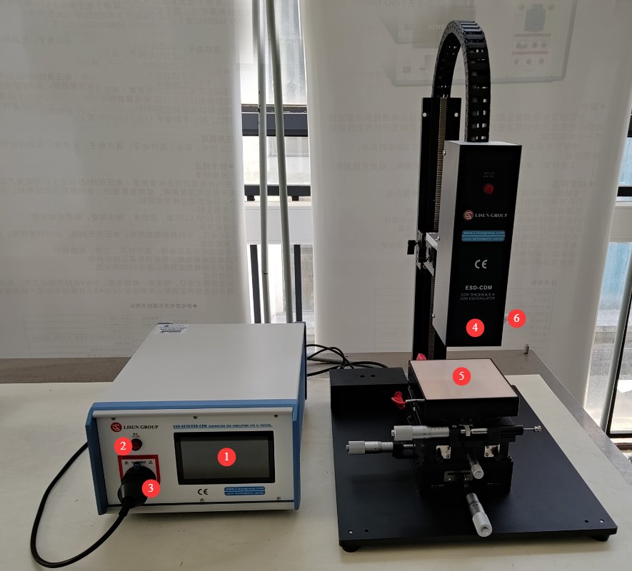
3.1 正面図
図3-1を参照してください。
| 数 | お願い |
|---|---|
| 静電気放電シミュレータ | |
| ① | タッチスクリーン |
| ② | 高電圧表示灯 |
| ③ | 高電圧接続。位置決めピンを持ち上げ、放電塔の高電圧プラグの溝を位置決めピンに合わせて、ゆっくりと奥まで差し込みます。その後、位置決めピンを下げて高電圧プラグを固定します。 |
| CDM Electrostatic Discharge Tower | |
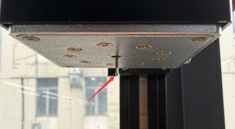
| ④ | Probe lift frame; the probe mounting location is directly opposite the test bench, as shown in Figure 3-2. |
| ⑤ | Standard test stand, adjustable for both position and height |
| ⑥ | BNC connector; use a coaxial cable to connect to an oscilloscope to view the output waveform. Note: Make sure the oscilloscope has a sufficient range, or use an attenuator to prevent damage to the oscilloscope. |
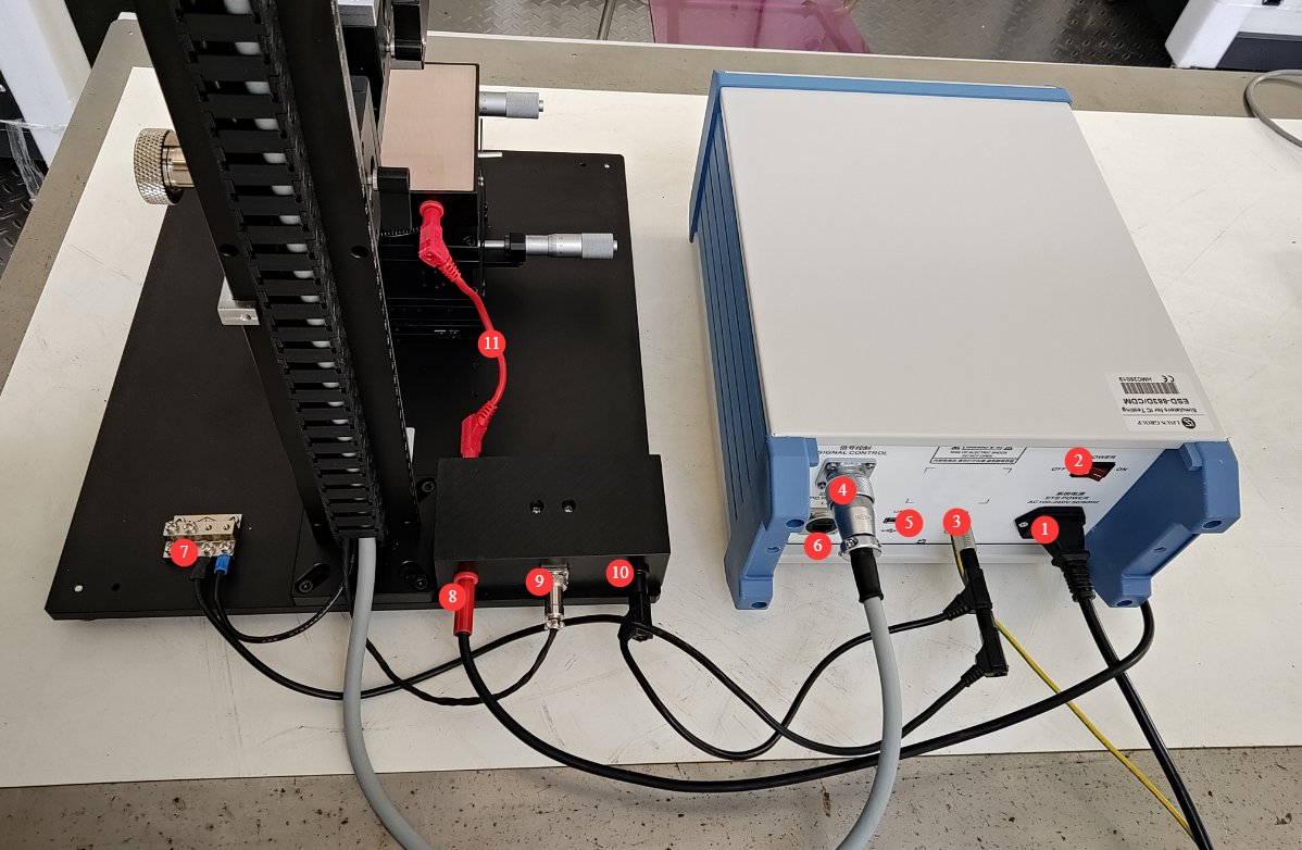
3.2 リアビュー
図3-3を参照してください。
| 数 | お願い |
|---|---|
| 静電気放電シミュレータ | |
| ① | 電源コード接続部(ヒューズ付き):機器を適切な電源に接続するためのもの |
| ② | 電源スイッチ |
| ③ | PGND:保護接地端子。接地線を使用して大地に接続します。 |
| ④ | Connecting the Signal Cables to the Discharge Tower |
| ⑤ | USBポート:タッチスクリーンを操作するためのUSBマウスを接続したり、ソフトウェアをアップデートするためのUSBフラッシュドライブを接続したりするのに使用できます。 |
| ⑥ | LANポート、予備 |
| CDM Electrostatic Discharge Tower | |
| ⑦ | Grounding busbar: Connect the ground wire from the probe lifting frame to the grounding busbar, and then use a wire to connect the grounding busbar to the protective grounding terminal on the back of the Electrostatic Discharge Simulator. |
| ⑧ | High-Voltage Line Connection |
| ⑨ | Signal Line Connections |
| ⑩ | Connect the test bench ground wire to the protective ground terminal on the back of the Electrostatic Discharge Simulator. |
| ⑪ | High-Voltage Cable Connections on the Test Stand |
3.3 Replacing the Discharge Tower
This Electrostatic Discharge Simulator can be connected to discharge towers used for various tests. If you need to replace the discharge tower for testing, please follow the operating procedures below strictly.
| 説明書 | お願い |
|---|---|
| ① | 静電気放電シミュレータが「テスト停止」状態になっていることを確認してから、シャットダウンしてください。 |
| ② | Disconnect all cables connecting the original discharge tower to the Electrostatic Discharge Simulator. |
| ③ | Connect all the cables between the new discharge tower and the Electrostatic Discharge Simulator. |
| ④ | Turn on the computer and run the new test. |
4. タッチスクリーンプログラムの概要
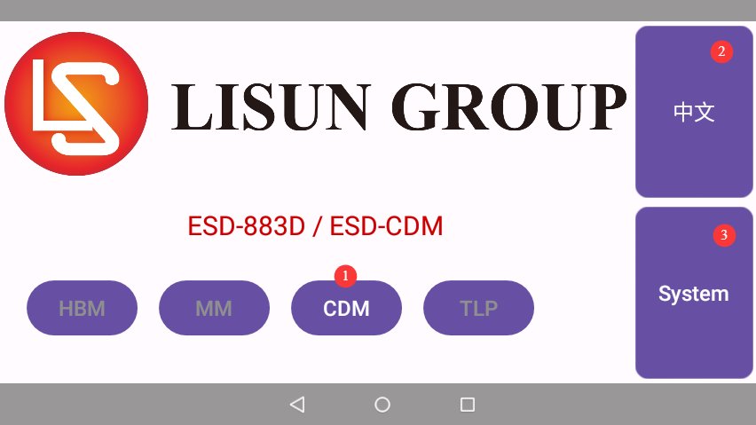
4.1 第一画面
図4-1を参照してください。
| 数 | お願い |
|---|---|
| ① | When the CDM discharge tower is connected to the host, “CDM Available” will be displayed; click it to enter the CDM test interface. |
| ② | 中国語と英語を切り替える |
| ③ | 製品情報ページ |
4.2 CDM Test Interface
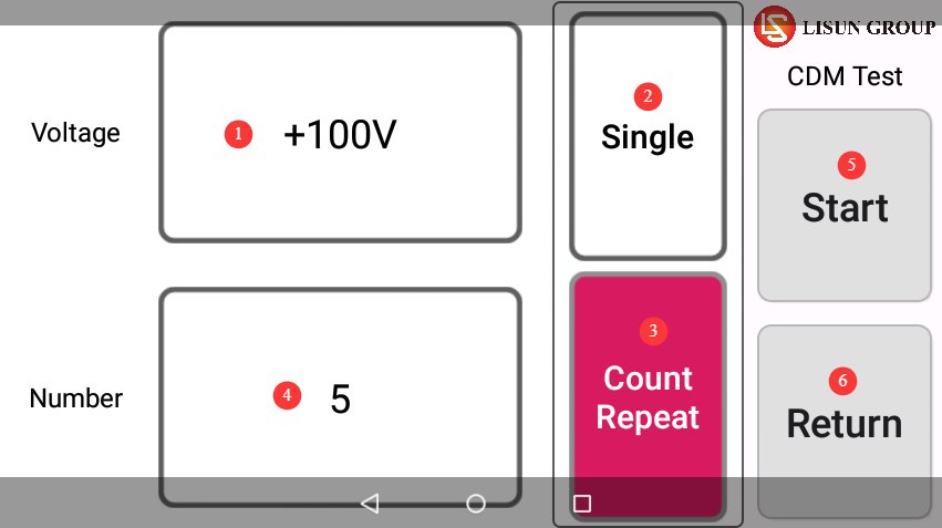
図4-2を参照してください。
| 数 | お願い |
|---|---|
| ① | 試験電圧と極性を設定できます |
| ② | 単一のテストを実行する場合は、「単一テスト」を選択してください。 |
| ③ | If you want to run continuous testing, select “Continuous Testing.” |
| ④ | You can set the number of tests; only consecutive tests are allowed. |
| ⑤ | テストの開始/停止 |
| ⑥ | ホーム画面に戻る |
5. CDM Electrostatic Discharge Testing
5.1 Preliminary Commissioning of the Test Bench Location
5.1.1 試験対象機器の配置要件
Operators should wear antistatic wristbands and antistatic clothing to prevent static electricity from the human body from damaging the devices under test; place the semiconductor devices under test with their pins facing upward in the center of the isolation plate,
5.1.2 Test Bench Commissioning
First, disconnect the high-voltage connection cables and place them on an insulated work surface. Then, refer to Section 4.2 to begin the test. Lower the probe at the standard speed. Based on the probe’s position as it descends, adjust the test stand’s height and horizontal alignment so that the probe makes just enough contact with the target pin upon reaching the bottom. Observe the contact status to avoid damaging the device pins due to excessive pressure. Once the adjustments are complete, stop the test and reconnect the high-voltage cable.
5.2 推奨される標準試験パラメータ
In accordance with the ANSI/ESDA/JEDEC JS-002-2014 standard, the recommended parameters for routine testing are as follows: Discharge voltage: Select based on device class—Class 0 (<250 V), Class 1 (250 V to <500 V), Class 2 (500 V to <1000 V), Class 3 (≥1000 V); Discharge polarity: Test once for both positive and negative polarities; Number of discharges: At least 3 discharges per pin.
5.3 テストの開始/停止
Set the test parameters as described in Sections 4.2 and 5.2, and start the test. If any abnormalities occur during the test, press the stop button to halt the test, make the necessary adjustments, and try again. After the test is complete, ensure that any internal residual charge is completely discharged, and remove the device under test. If the equipment will not be used again that day, you may turn it off.
5.4 テスト結果の解釈
すべての規格は、統一された試験および評価ロジックに従っています。
| 数 | お願い |
|---|---|
| ベンチマーク | Before the CDM discharges, measure all parameters under the conditions specified in the standard and record the reference values. |
| 放電テスト | Perform CDM discharges at the specified voltage, polarity, and number of cycles as required by the standard |
| Comparison of Retest Results | After discharge, remeasure all parameters under conditions identical to those used for the baseline test. |
| 故障判定 | いずれかのパラメータが仕様値を超えた場合、デバイスが誤動作した場合、または物理的な損傷が生じた場合、試験対象デバイスは不合格とみなされます。 |
| レベル確認 | The highest voltage at which none of the samples failed shall be used as the final CDM withstand rating for the device under test. |
6. 機器の日常的なメンテナンスと手入れ
6.1 毎日の清掃とメンテナンス
After each test, use a clean, soft cloth to wipe dust from the main unit’s exterior, the touchscreen, and the surface of the discharge tower to keep the equipment clean; use a dedicated screen-cleaning cloth to clean the touchscreen. Do not use organic solvents such as acetone, and do not spray water directly onto the screen to clean it; Clean dust and foreign objects from the surfaces of the test bench, sensing plate, and isolation plate weekly to ensure good insulation performance; if the probe tip is soiled, gently wipe it with a lint-free cotton swab dipped in a small amount of anhydrous ethanol, and allow it to air dry before use.
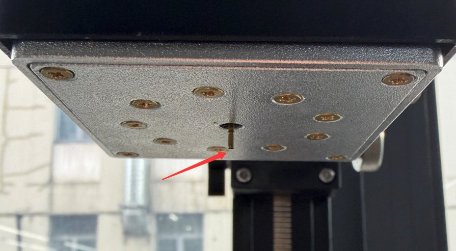
The probe can be unplugged directly for cleaning or replacement; see Figure 6-1.
6.2 Items for Periodic Inspection
6.2.1 電気接続の点検
Inspection Frequency: Once a month; Inspection Items: Check power cords, high-voltage cables, grounding wires, and communication cable connectors for looseness, oxidation, or damage; Remedial Actions: Tighten any loose connectors immediately; gently sand off any oxidation with fine-grit sandpaper; and replace any damaged cables immediately.
6.2.2 機械構造物の検査
Inspection Frequency: Once a month; Inspection Items: Check whether the test bench adjustment knobs turn smoothly, whether the probe bracket stop blocks are secure, and whether the probe extends and retracts normally; Remedial Actions: Apply a small amount of silicone grease to the adjustment mechanism for lubrication; replace the probe if it is deformed or worn.
6.3 長期保管要件
Before long-term storage, clean the entire surface of the unit and unplug all external cables; cover the unit with a dust cover and store it in a dry, well-ventilated environment free of corrosive gases; the storage environment should have a temperature of 0°C to 40°C and a relative humidity of ≤70%, and direct sunlight should be avoided; Every 3 months, power on the device and leave it in standby mode for 30 minutes to remove moisture and protect the high-voltage modules.
6.4 校正間隔の要件
機器の測定精度と動作信頼性を確保するため、定期的に認定された第三者計測機関に送付して校正を受けることを推奨します。推奨される校正間隔は12ヶ月です。具体的な校正間隔は、使用頻度、環境条件、および品質システム要件に基づいてユーザーが決定できます。
7.よくある問題のトラブルシューティングと解決
7.1 電源関連の障害
| 障害症状 | 考えられる原因 | 手順 |
|---|---|---|
| No display when powered on; power indicator light does not turn on | 電源コードがしっかり差し込まれていません。ヒューズが切れています。 | Check the power cord connections; replace the fuse with one of the same rating after turning off the power. |
| タッチスクリーンが反応しない | 画面に汚れがあり、システムが正常に動作していません。 | 画面表面を清掃し、デバイスを再起動してください。 |
7.2 高電圧故障
| 障害症状 | 考えられる原因 | 手順 |
|---|---|---|
| High voltage cannot be applied after clicking “Start.” | High-voltage cables not properly connected, poor grounding, and dirt on the test bench surface | After turning off the power, unplug and replug the high-voltage cables, then tighten them; check and secure the ground wire; clean the surface of the test bench. |
7.3 動作上の不具合
| 障害症状 | 考えられる原因 | 手順 |
|---|---|---|
| Discharge cycles are not counted | The probe is not in contact with the device | Recalibrate the position to ensure good contact. |
| Communication error; the discharge tower is not operating | 通信ケーブルの緩み | Tighten the signal cable connections after power is turned off |
7.4 Waveform Anomalies
| 障害症状 | 考えられる原因 | 手順 |
|---|---|---|
| The waveform peak is too low | Poor probe contact, voltage set too low | Clean the probe tip and adjust the contact pressure; verify and increase the set voltage. |
| The rising edge of the waveform does not meet specifications | Probe wear, excessive ground loop impedance | Replace the test probe; check the ground wire and reduce the ground resistance. |
| Many waveform artifacts | Electromagnetic Interference from the Surroundings | Eliminate sources of interference and use shielded cables |